

Ultrafast self-sintering of silicon nanoparticles into highly porous material for batteries, electronics, and sensors.
Ultrafast self-sintering of silicon nanoparticles into highly porous material for batteries, electronics, and sensors
BACKGROUND
We offer a new route to fabricate highly porous silicon-based nanostructures at scale using a one step, fast, and highly reproducible process of explosive sintering of nanoparticles, compatible with heat-sensitive substrates such as paper. The problem addressed is that conventional porous silicon processing often relies on high-temperature annealing, etching, multi-step treatments, or poorly controlled sintering routes. These approaches have increased cost, energy demand, processing complexity, and limited control over porosity, crystallinity, and grain connectivity. Our invention in turn is a bottom-up sintering route in which silicon-based nanoparticles are deposited as a granular structure and then fused together in less than a second using explosive oxidation triggered under ambient or near-ambient conditions. The output is a mixed-phase silicon-based nanostructured material with larger interconnected grains and high porosity. The technology is at TRL 4, with laboratory validation of the process and material characteristics demonstrated, and is now suitable for industrial co-development, licensing, and scale-up assessment. Focus industries include battery manufacturing, semiconductor and thin-film electronics, sensors and biosensors, optoelectronics and photonics, catalysis, and printed materials.
Key points of differentiation include the fast speed of the reaction, the fact that it only takes an ignition step to get the sintering reaction to occur in all the target material, sintering being low-temperature and not using a furnace, as well as having controlled trigger of sintering, achieving the bottom-up formation of larger interconnected mixed-phase grains rather than isolated nanoparticles, having less wasted material, and being compatible with heat-sensitive substrate deposition, coatings, films, or powder-like porous structures. Morphological and chemical analysis reported in the patent confirms increased crystallinity, grain growth, and macroporous morphology after sintering.
Industrial applications include: lithium-, sodium- and potassium-ion battery anodes; silicon-rich energy-storage composites; thin-film electronics; semiconductor and microelectronic materials; MEMS/NEMS structures; chemical and biosensors; optoelectronic devices; photonic or light-emitting porous silicon systems; catalyst supports; hydrogen- or gas-reactive porous materials; functional coatings; printable or deposited silicon films; and high-surface-area silicon platforms for advanced materials R&D.
What advantage does this process offer? This method is a lower energy, faster, controllable, and potential cheaper route to obtain highly porous silicon nanostructures with tunable material morphology. Can it scale? We have proven sintering is highly reproducible in areas of up to 10 cm2 and can be readily scaled to larger dimensions, since it is limited only by the availability of silicon nanoparticles and ambient air rather than fundamental limitations of the sintering mechanism itself. Is it application-ready? Being at TRL 4, the process has been validated in laboratory, with testing in devices, electrodes, coatings, or process lines to come. What is the competitive landscape? Existing porous silicon manufacturing routes include electrochemical etching of silicon wafers, thermal annealing of silicon nanoparticles, CVD/plasma deposition, laser processing, and chemical synthesis of silicon nanostructures. This invention is differentiated by combining nanoparticles with trigger-induced self-sintering to obtain porous mixed-phase silicon quicker, with less material waste, and without conventional high-temperature bulk processing which makes it compatible with temperature sensitive substrates.
TECHNOLOGY OVERVIEW
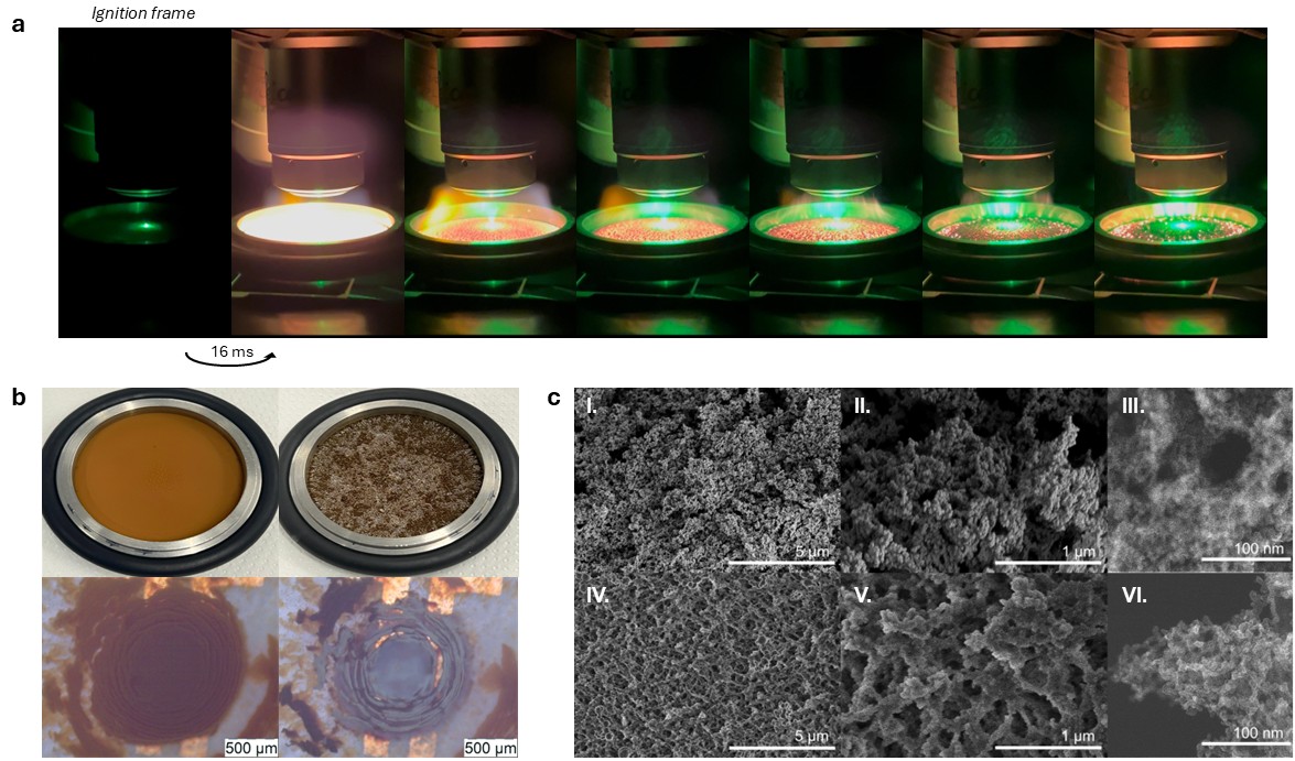
The invention consists of leveraging silicon’s high affinity to binding with oxygen exothermically to sinter silicon nanoparticles together using a combustion reaction. For this, we need nanometer-scale hydrogen-terminated particles of silicon or silicon-based materials to be packed together to a certain optimal degree in which the nanoparticles are near one another and at the same time still maintaining enough space for ambient air to be present between them. The hydrogen covering the nanoparticles acts as a barrier between the oxygen in ambient air and the underlying silicon. The high surface-to-volume ratio of nanoparticles allows for the reaction to propagate much more and give out enough energy to fuse the particles, which also melt at lower temperature at these sizes. An external trigger is needed to locally remove several hydrogen terminations at once and start the reaction. This trigger can be a physical impact, and electrical spark, the light of a laser, among others. As soon as the hydrogen in the surface of the nanoparticles is removed, the oxygen in air will want to bond with silicon, and by doing so it releases a lot of energy which in turn breaks more adjacent surface hydrogen bonds, exposing more silicon to oxygen, creating a self-sustained combustion reaction that propagates throughout the whole material. The nanoparticles melt and fuse together, forming a highly porous Si material consisting of interconnected grains several times larger than the nanoparticles, each made up of silicon nanocrystals embedded in an amorphous silicon and silica phase. The reaction occurs very fast locally and can cover areas of 10 cm2 in under 30 milliseconds. The degree of packing and the size of the nanoparticles influences the morphology, pore size, and grain size of the sintered material. Since the reaction is self-sustained, it is only limited by the availability of silicon nanoparticles, ambient air, and a trigger action. By applying this explosive sintering to Si-NPs deposited on patterned paper substrates to create field-effect transistors, the sintered material was found to behave as an n-type semiconductor.
STAGE OF DEVELOPMENT
TRL 4 – with laboratory validation of the process and material characteristics demonstrated, and is now suitable for industrial co-development, licensing, and scale-up assessment.
BENEFITS & APPLICATIONS
This new method to create a highly porous mixed-phase silicon-based material material can be leveraged by industries for applications where a porous scaffold or specifically porous silicon is of interest. The key characteristics of the manufacturing method are that it is a very fast (millisecond-second range) bottom-up process that is self-contained and self-sustained, allowing for full sample conversion provided there are sufficient silicon nanoparticles to convert and ambient air or another oxidizing atmosphere is available. This translates into a lower energy, faster, controllable, and potential cheaper route to obtain highly porous silicon nanostructures with tunable material morphology. Some examples of industries that can benefit of such method are:
Battery manufacturing: Porous silicon architectures could be used in Li-ion, Na-ion, K-ion, and solid-state battery anodes. Silicon has extremely high theoretical capacity, but major failure modes include large volume change, pulverization, SEI instability, and loss of electrical contact. A porous interconnected structure could help accommodate anode expansion, reducing anode pulverization while improving electronic percolation, greatly increasing battery capacity in the process.
Semiconductors and thin-film electronics: The method offers a lower-temperature and possibly more cost-effective route to polycrystalline silicon-based films or coatings, relevant to TFTs, sensors, MEMS, and substrate-integrated silicon structures. Moreover, the lower thermal budgets of the method enable integration on substrates that cannot tolerate conventional high-temperature processing, as we have demonstrated by creating paper-based field-effect transistors with sintered Si-NPs working as active material.
Sensors and biosensors: Porous silicon is attractive because high internal surface area can improve sensitivity while leveraging the semiconductor nature of silicon in optical, chemical, and biosensing formats. It can also be tailored to be bioactive or bio inactive.
Optoelectronics and photonics: Porous silicon is already studied for photoluminescence, optical sensing, photonic structures, and refractive-index-engineered materials. Local trigger-controlled sintering enables patterned porous silicon structures without full-wafer thermal treatments and with compatibility with underlying devices or substrates, even if they are less thermally stable (e.g. paper).
Catalysis and functional supports: The high-surface-area silicon network could function as a support for catalytic, photocatalytic, or electrocatalytic materials. Again, the lower thermal budgets of the method enable integration on substrates that cannot tolerate conventional high-temperature processing.
Functional coatings and printed/deposited materials – leveraging localized and patterned nanoparticle depositions followed by triggering, means we can achieve patterned coatings, perform additive manufacturing, or create silicon-based functional layers.
The main competing technologies are electrochemical etching, metal-assisted chemical etching, thermal annealing/sintering of silicon nanoparticles, and CVD/PECVD-based silicon film deposition. Conventional porous silicon is often produced by wet etching of silicon wafers, frequently involving hazardous top-down HF acid etching chemistry and wafer-format processing, while metal-assisted chemical etching also depends strongly on substrate, catalyst, etchant, and process conditions.
This invention is differentiated because it is a bottom-up process rather than subtractive. Instead of etching pores into a wafer, it builds a porous silicon network from nanoparticles. That reduces dependence on expensive and energy intensive crystalline silicon wafers, allows for coating of different substrates, and enables more flexible geometries. It also leverages readily triggered sintering even on top of heat-sensitive substrates like paper, avoiding high-energy processing like in furnaces. This is important for flexible electronics, temperature-sensitive substrates, and lower-energy manufacturing.
The other major advantage is structural since using just silicon nanoparticles typically results in poor electrical connectivity and instability. A porous polycrystalline network can combine the benefits of nanoscale porosity with better grain-to-grain connectivity, as demonstrated in the paper-based field-effect transistors due to their relatively high carrier mobility. For batteries, this could address expansion, cracking, and loss of contact. For sensors, it could preserve high surface area while improving mechanical and electrical robustness.
INTELLECTUAL PROPERTY
- Patent submitted
OPPORTUNITY
- Available for exclusive and non-exclusive licensing
- Seeking co-development partners and/or Sponsored Research
FURTHER DETAILS
Figure 1 – a) Frame by frame look at the laser ignition of the explosive sintering of silicon nanoparticles. Upon triggering, the reaction wave propagates throughout the whole 10 cm2 sample in less than 32 ms. b) images of the silicon nanoparticle (left) before and (right) after sintering, resulting in (top) branch-like and (bottom) sponge-like macroporous nanostructures. c) Morphological characterization of sintered materials. I,II, SEM images of sintered samples showing branch-like macroporous networks; III, bright-field TEM of individual grain in branch-like network revealing its internal nanoporous structure; IV,V, SEM images of sintered samples showing sponge-like macroporous networks; VI, bright-field TEM of individual grain in sponge-like network revealing its internal nanoporous structure.
NOVA Inventors
Hugo Águas
João Mendes
Luís Pereira
Diana Gaspar
Rodrigo Martins
